Ferromagnetic semiconductors such as p-type (Ga,Mn)As are well suited for investigating the interplay between magnetic domains and electronic carriers, since both the growth of III-V semiconductor heterostructures and the fabrication of electrical devices is well established via molecular beam epitaxy (MBE) and nano-lithography, respectively. In order to pin and probe magnetization domains at a given position on a Hall-bar, the effective anisotropy energies of the crystal need to be controlled on a mesoscopic level.
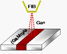
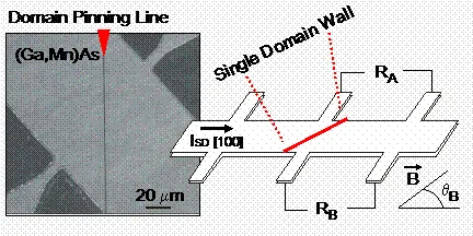
We use a focused ion beam (FIB) of Ga+ ions to imprint domain pinning centers at specific locations along a patterned Hall mesa of a (Ga,Mn)As epilayer [1]. These nonmagnetic defects increase the local magnetic anisotropy energies, by which a domain wall is pinned at a given position.
The devices studied are Hall bars patterned on the magnetic epilayer of the (Ga,Mn)As samples. The pinning lines are defined with an FIB across one set of Hall probes (see red line in the figure below). When a domain wall is pinned at this line, a comparison between the resistances RA and RB yields insight into the domain wall dynamics at the pinning line, while the difference between RA-RB eliminiates the resistive bulk contribution of the epilayer.
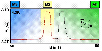
Sweeping an external magnetic field in-plane yields two hysteretic jumps in the resistance trace (see figure below). This behavior is a signature of the giant planar Hall effect [2] and can be explained by quasi-particle scattering from ionized Mn2+ acceptors. The anisotropic magnetoresistance allows us to read out the directions M1, M2 and M3 of the magnetic domain. Since these easy axes of the magnetization are found in-plane (close to <100>), any artifacts due to the anomalous Hall effect are minimized. Because the external magnetic field is also applied in-plane, the normal Hall effect is zero.
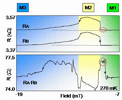
In (Ga,Mn)As epilayers, changes in the global magnetization are driven by the passing of a 90 degree domain wall. The figure below demonstrates how a domain wall is caught at the pinning line [1]. Just before the magnetization jumps globally into the M2 state, RA features a small resistance increase (red circle) which is due to a local magnetization reversal at the pinning line. By measuring the resistance difference RA-RB we are able to monitor the passing of the domain wall with greater resolution (lower graph).
This experimental technique allows us to probe and manipulate domain walls in ferromagnetic semiconductors individually [1],[3]. In addition, we can extract the intrinsic resistance of such a macroscopic domain wall [4]. Generally, the reported pinning phenomena can be seen at temperatures below the Curie temperature (71K).
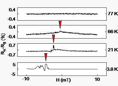
The featureless character of the top trace above TC demonstrates that the resistance residue which is detectable below TC is a signature of the ferromagnetic properties of (Ga,Mn)As [3]. For lower temperatures, the peak center (red triangle) occurs at progressively more negative field amplitudes, which is consistent with thermally nucleated domain walls.
For more information please refer to:
- [1] A. W. Holleitner, H. Knotz, R. C. Myers, A. C. Gossard, and D. D. Awschalom, Appl. Phys. Lett. 85, 5622 (2004).
- [2] H. X. Tang, R. K. Kawakami, D. D. Awschalom, M. L. Roukes, Phys. Rev. Lett. 90, 107201 (2003).
- [3] A. W. Holleitner, H. Knotz, R. C. Myers, A. C. Gossard, and D. D. Awschalom, J. Appl. Phys. 97, 1 (2005).
- [4] H. X. Tang, S. Masmanidis, R. K. Kawakami, D. D. Awschalom, and M. L. Roukes, Nature 431, 52 (2004).