Some of the strengths of the silicon carbide is its availability at the wafer scale, doping control, and device fabrication that makes it a promising solid-state platform for quantum information processing and quantum sensing. In our result, we leverage these strengths by integrating our isolated, single quantum emitters, the neutrally-charged divacancy (VV0), in a diode and demonstrate massive optical tunability as well as dramatic optical linewidth narrowing.
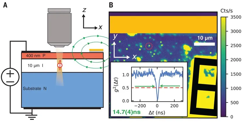
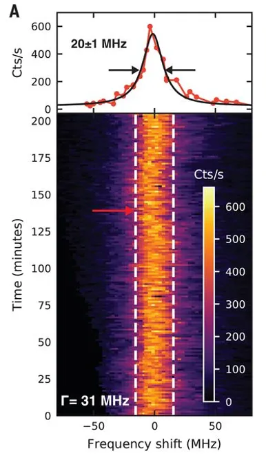
Fluctuating charges in the host material of a defect can cause unwanted fluctuating electric fields that can cause dephasing that results in spectral diffusion and large broadening of the optical linewidths. When reverse bias is applied to the diode, large electric fields are generated that cause charge depletion of the intrinsic region of the device. This charge depletion results in the narrowing of the optical linewidths of the VV0 by more than 50-fold of its original linewidth.
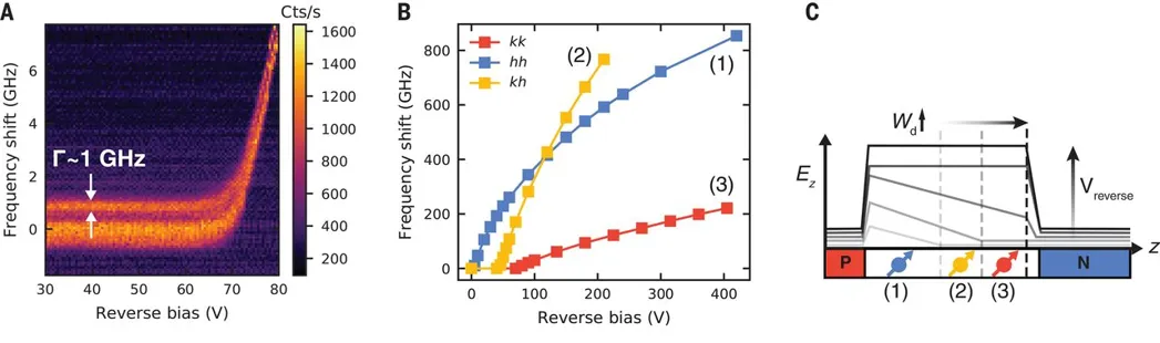
From the applied bias, large Stark shift tunability of axial-oriented VV0 optical resonance frequency is observed for greater than 850 GHz. The thin i-type region (10 um) of the diode enables a large Stark shift of the defect. We are able to apply large voltages with low currents across the diode, up to 420 V, in reverse bias to tune the defect because of its rectifying behavior at cryogenic temperatures.
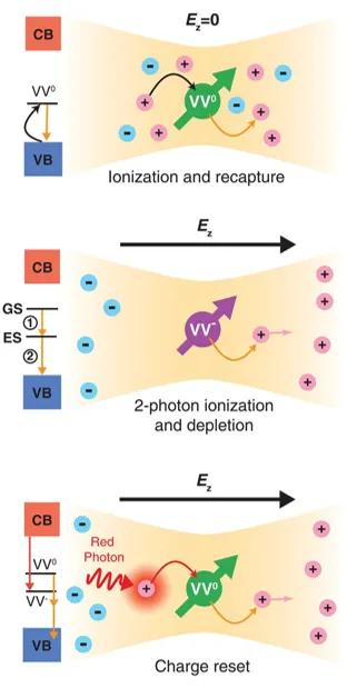
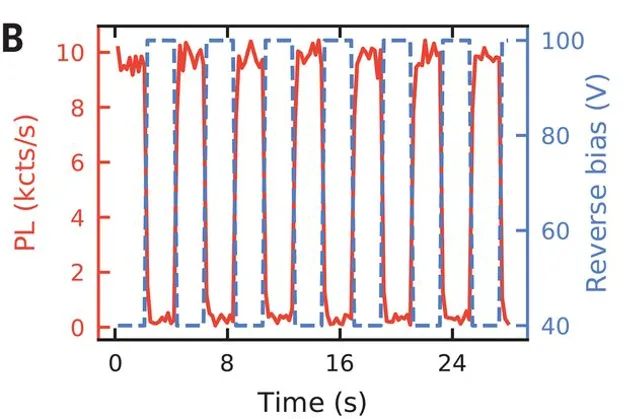
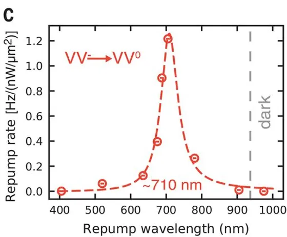
All of these observations in the diode are enabled by the understanding and control of the charge dynamics via applied electric fields. We observe a substantial drop in the photoluminescence (PL) when an offresonant 975-nm light is applied in conjunction with a reverse bias past the defect’s threshold, depending on the defect’s depth in the intrinsic region. We attribute this reduction in PL to photoionization of the defect to an optically dark charge state. We are able to create an electrically gated single-photon source from this photoionization understanding. Furthermore, we were able to find the ideal wavelength (~710 nm) under reverse bias to repump the VV0 into the correct charge state that emits light from its dark one.
Details can be found in our manuscript: