Incorporating photonic control into silicon carbide spin systems offers a scalable pathway towards enabling quantum information and sensing applications. By fabricating carefully designed photonic crystal cavities in the vicinity of silicon carbide divacancies, we can enhance the emission of light from these defects under optical excitation. This emitter-cavity coupling and enhancement is given by the Purcell factor:

Where λcav is the resonant wavelength of the cavity, n is the refractive index of the cavity material, Q is the quality factor of the cavity, and Vmode is the mode volume of the cavity mode. Thus, the highest enhancements come from structures with high quality factors and low mode volumes. This is the maximum spontaneous emission enhancement, where losses can occur from imperfect overlap between the emitter and cavity mode, as well as mismatch between the emitter and cavity resonant wavelengths. With respect to emission rates, the Purcell factor can be expressed as:

Where Γ0 is the spontaneous emission rate of the emitter in free space and Γg is the modified emission rate.
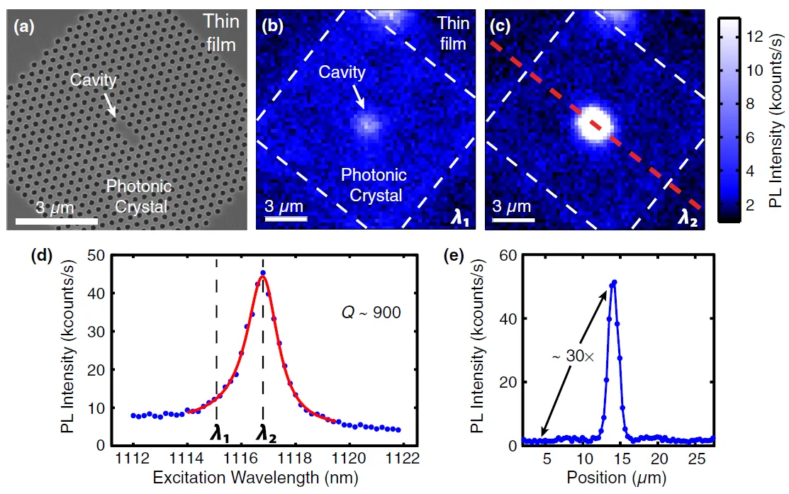
In our experiments we have fabricated photonic crystal cavities that maximize the Purcell factor and thus the corresponding emission rate of the embedded divancanies. More specifically, we have focused on thin film photonic crystal slabs in 3C-SiC with integrated ky5 divacancy ensembles. The 3C polytype can be epitaxially grown on a silicon substrate, allowing for an undercut and the formation of higher quality suspended photonic crystals. As shown in the above figure, photoluminescence (PL) intensity is significantly increased when the excitation wavelength matches the cavity resonant wavelength. Cross-polarized excitation measurements have yielded quality factors on the order of ~900, with a ~30 increase in PL intensity in a cavity mode volume of roughly ~(λ/n)^3.
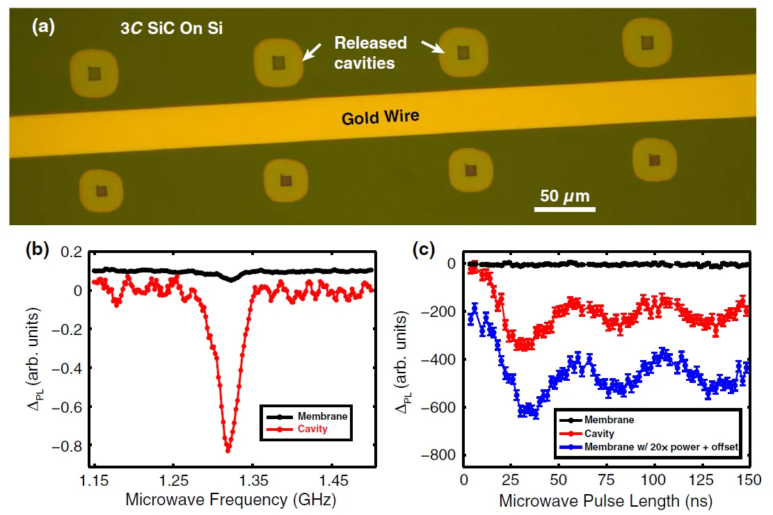
In addition to enhancing PL intensity, photonic crystals have also been shown to increase signal contrast in optically detected magnetic resonance (ODMR) scans and roughly double spin initialization rates. This results in much stronger ODMR peaks, equivalent to a ~20x increase in microwave power. In the above figure, a photonic crystal cavity array is positioned 50 microns from a gold stripline for driving microwaves. Subsequent continuous ODMR scans at 1.319 GHz are shown in (b), and pulsed ODMR scans in (c).
The divacancy signal enhancements provided by photonic crystal cavities span a broad range of applications. Increasing PL intensity, especially in the zero-phonon line (ZPL), is a key component in enabling scalable photon-heralded entanglement schemes for quantum communication. Effective increases in microwave power would aid on-chip applications such a spin-based sensing. Cavity-emitter coupling would also enhance optical stark shifts, single photon frequency conversion, and single-photon source performance.
To learn more about our work, please see:
“Silicon carbide photonic crystal cavities with integrated color centers”, G. Calusine, A. Politi, and D. D Awschalom, Appl. Phys. Lett. 105, 011123 (2014)
“Cavity-enhanced measurements of defect spins in silicon carbide”, G. Calusine, A. Politi, and D. D. Awschalom, Phys. Rev. Applied 6, 014019 (2016)