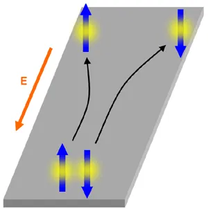
When a conductor is subject to crossed electric and magnetic fields, a charge current transverse to both the applied fields appears as a result of the Lorentz force. Discovered more than 100 years ago, this is known as the Hall effect which has lead to many important findings in solid-state systems, and still finds applications in magnetic field sensors today. In an analogy to the conventional Hall effect, the spin Hall effect refers to a pure spin current transverse to an applied electric field in the absence of applied magnetic fields, and was theoretically predicted more than 30 years ago (see schematic below). A pure spin current is a flow of spin angular momentum without any charge current, which can be realized, for example, by spin-up and spin-down electrons moving in opposite directions. At the edges of a sample, the spin current results in accumulation of spins, similar to charge accumulation in the conventional Hall effect. We use Kerr microscopy to detect and image such spin accumulation.
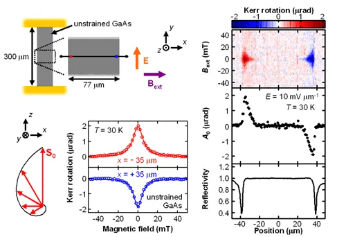
First, we look at an ustrained GaAs sample. It is fabricated from 2 microns of n-GaAs grown by molecular beam epitaxy, into a channel of width 77 microns and length 300 microns. Under the application of electric field, Kerr rotation is measured as a function of magnetic field at two positions: left edge, indicated by a red spot, and right edge, indicated by a blue spot. We observe Lorentzian curves, indicating out-of-plane spin polarization (Hanle effect). The polarization changes sign for the two edges, consistent with the spin Hall effect. We take such data across the channel, and observe that the polarization is localized at the edges.
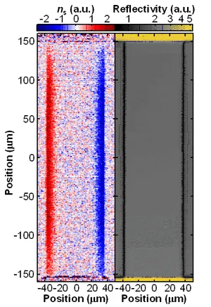
It is also possible to image the spin polarization. The figure below shows the image of the spin polarization as well as just the reflectivity. The spin accumulation is evident over the whole sample.
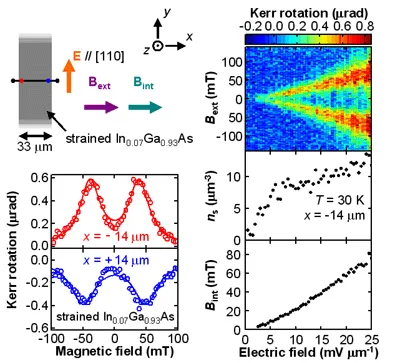
Now we turn to a strained InGaAs sample. Strained InGaAs shows spin precession without magnetic fields, due to the internal magnetic field. The magnetic field scans now show two peaks. This is caused by the internal magnetic field. Finite external field is needed to cancel the internal magnetic field, so the peak is offset from zero. In addition, measurement scheme requires modulation of electric field (in this case a square wave is applied to the contacts,) and therefore two peaks appear, corresponding to positive and negative electric fields.
Such an interpretation is justified by looking at what happens as a function of electric field. The peak splitting increases with electric field, consistent with previous results.
To learn more about our studies, please refer to "Observation of the spin Hall effect in semiconductors", Y. K. Kato, R. C. Myers, A. C. Gossard, and D. D. Awschalom, Science Express 1105514 (2004)