Defects in solid state materials have different charge states. These charge states often have different emission characteristics - they may have different emission spectra or no photoluminescence (PL) at all, as opposed to the charge states more commonly studied. We can efficiently move between charge states of different defects using optical pumping. The rate of this charge state conversion using optical pumping in both the silicon vacancy and the divacancy (VV) in SiC depends on the presence of electric fields. Therefore, we can detect applied RF fields using changes in the PL of the defects, which is electrometry by optical conversion (EOCC). We observe change in the PL of VV over time depending on the magnitude of the applied electric field by measuring R, the characteristic decay time.
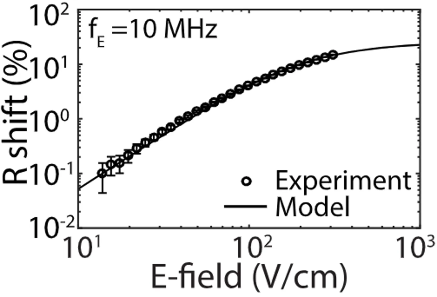
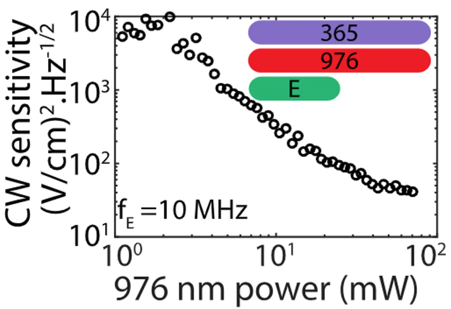
For an electric field frequency of 10 MHz, we can obtain sensitivity of down to 41 (V/cm)^2/sqrt(Hz) with an ensemble of approximately 10^4 VVs.
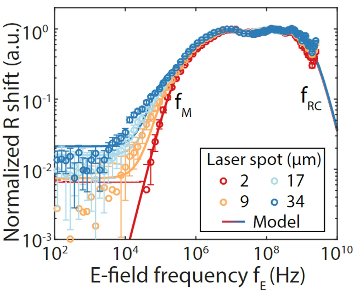
We also observe shifts in R depending on the frequency of the applied electric field. This shows that EOCC can work for frequencies up to a few GHz.
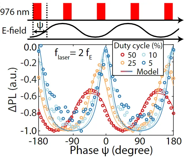
We can also measure the phase of the electric field using the change in PL.
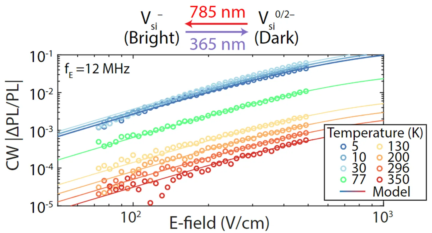
By using the same general technique, we can see how changing the magnitude of the electric field changes the PL response of the silicon vacancy defect as well.
Since SiC is piezoelectric, this electrometry technique can also be used to map mechanical strain in the material. We can fabricate a surface acoustic wave (SAW) resonator, which will have particular transverse wave modes. Using EOCC, we can directly observe these transverse modes and are able to fully separate each mode in both the spatial and frequency domains.
We build off our previous work by using heterodyne electrometry measurements. We design a system with two sets of electrodes, one for a pump electric field and one for the sensed electric field. When the lock-in detection frequency matches the frequency difference between the pump and sensed electric fields, we obtain a signal that is proportional to the product of the magnitudes of the two electric fields. Using this, we can observe how the EOCC contrast changes as a function of the sensed electric field magnitude, for both coherent and incoherent heterodyne measurements.
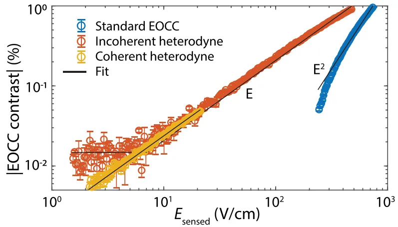
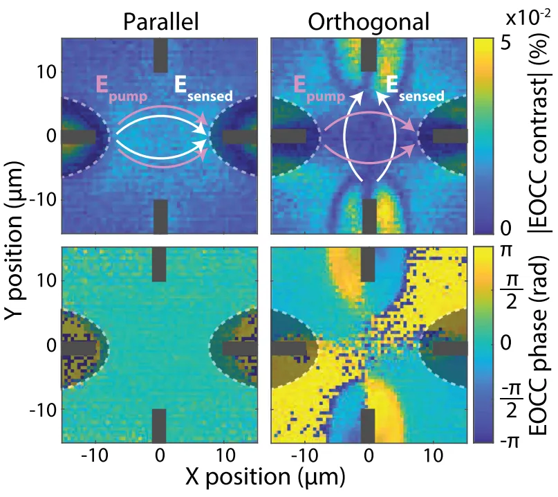
The best sensitivity reached is 1.1 (V/cm)/sqrt(Hz), which is slightly better per defect than sensitivity achieved for a single spin and two orders of magnitude better per defect for a large ensemble. Furthermore, we can apply the pump electric field both parallel and orthogonal to the sensed field. Since the signal is also proportional to their dot product, we can map out the vector components of the electric field in a 2D map.
Details can be found in our manuscripts: